RG1 – CMOS-RRAM Analog Integrated Circuits for AI Accelerators
Machine learning (ML), especially deep learning (DL) algorithms, has been evolved rapidly as one of the main pivotal topics in artificial intelligence (AI) and has been proven to be a remarkably powerful tool in a wide spectrum of intelligent information processing applications e.g. image and speech recognition. DL systems are built on the basis of bio-inspired computational models which requires driving a large number of connected computing units in parallel. These systems need a large amount of data for training and processing and to unlock their potential specialized DL hardware needs to be developed.
Conventional computing platforms, specially von-Neumann-based computing architectures, are seriously suffering from the limited data bandwidth between processing units and memory which makes them incompatible for big data processing and implementing state-of-the-art ML algorithms with extensive large sets of parameters. Also, from the technology point of view, complementary metal-oxide-semiconductor (CMOS) technology scaling is reaching its limits based on Moore’s law, and designing an ultra-efficient computing platform requires a scalable device that has the potential to reach higher density than the current CMOS footprint. Therefore, efficient design for specialized AI hardware will be deciphered by exploiting emerging technologies toward new computing paradigms and benefiting from software innovations to maintain a balance for both functionality and performance.
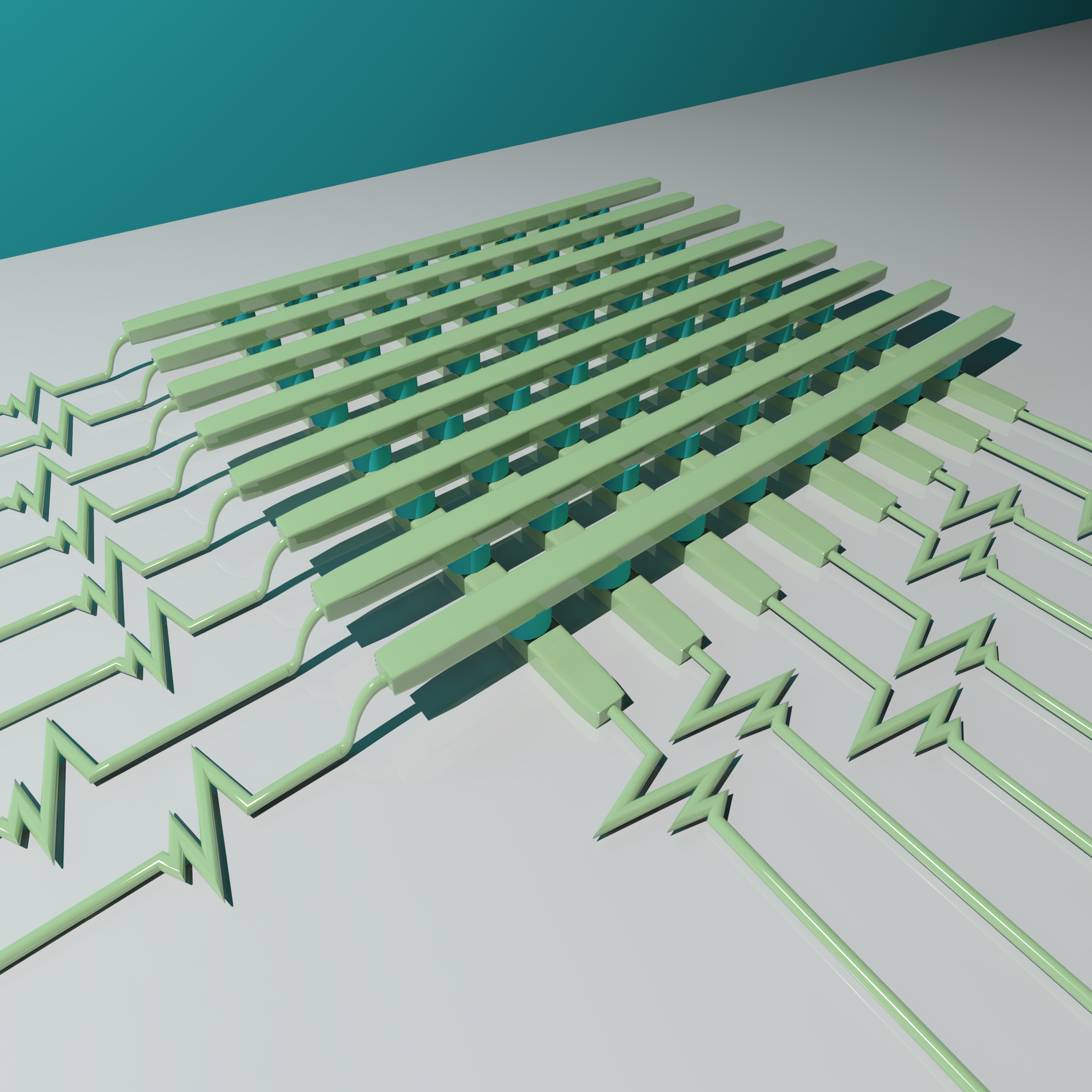
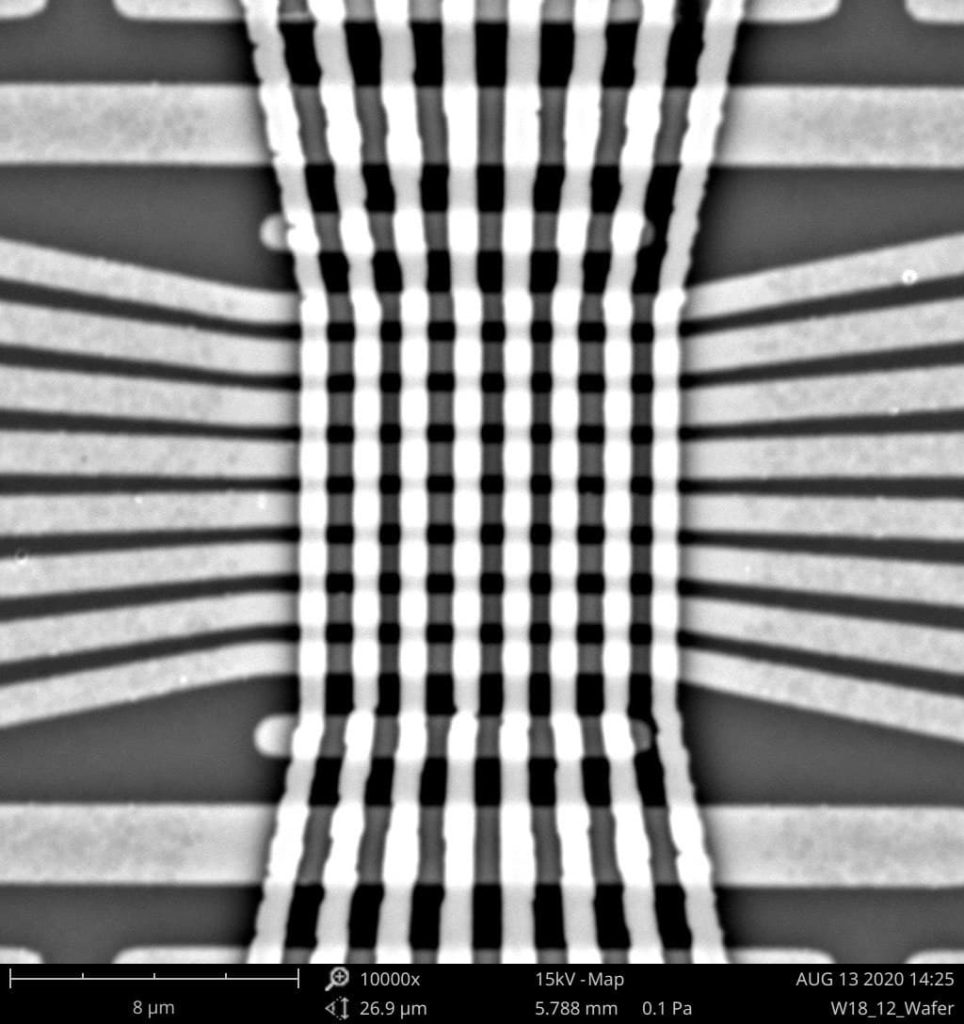
In this research stream, we will implement a scalable, flexible, and innovative strategy for the implementation of the synaptic weight and the associated multiply and accumulate (MAC) operation, one of the most demanding operations for efficient ML hardware. We will achieve an optimum balance between CMOS flexibility /performance and the density/energy efficiency of computation in emerging memory devices (resistive memory synapses). This will take place at two levels of integration: (i) we will use an advanced system-in-package approach in order to optimize heterogeneous integration of memory devices on CMOS chips. (ii) We will implement a massively parallel and dense memory array via multiple passive crossbar interconnection in a system-on-chip strategy. Active amplification between passive crossbars will enable ultra-high memory density while preserving optimal control of the memory devices. This project involves mixed-signal CMOS integrated circuits that enable in-memory computing architectures such as those using RRAM (resistive RAM), with the focus on densely integrated ADC and DAC design (the ADCs and DACs will control read and write operations for the RRAM). Topics may also include massively parallel analog computing architectures, computation in SRAM / DRAM, charge-domain signal processing, analog-to-information converters, analog-to-time converters, computational ADCs, multiplying ADCs, bit-level/bit-serial processing, reconfigurable architectures, and non-uniform sampling ADCs. Another aspect of this project is energy-efficient computing architectures relying on memristor arrays for machine learning algorithms (e.g., support vector machines, deep learning, boosting, ensemble methods.
Interested applicants for this research group can have more info about the requirements and qualifications details by clicking on the following button:

RG2 – Neuromorphic Computing Hardware
Based on the hardware power efficiency road map, in order to evolve toward more energy-efficient computing systems, there is a need to shift toward a bio-inspired and neuromorphic computing paradigm. Therefore, embracing a spike-based neural accelerator by using low-resolution memory cells will provide more energy-efficient systems in comparison with its ANN counterparts. Spiking neural network (SNN) is replaced by the ANN as the encoded sparse spike voltages are replacing continuous analog voltage inputs. A spiking version of VMM based accelerators has been also presented by offering much more energy efficiency while sacrificing the processing time. One of the major problems of such systems is the issue of sneak path current during main inference, tuning, and training operations which has been addressed through adding access devices like CMOS transistors, diodes, and selectors. Sneak path currents deteriorate the performance and accuracy of the RS-based VMM accelerators and avoiding it requires spending more area toward adding selector devices. A new class of RRAM devices has been introduced for the 0T1R structure with a high area efficiency feature and low sneak path current flow. These TiOx-based devices have been developed at Lille university by Dr. Fabien Alibart and will be available for experimental testing for neuromorphic applications.
We will explore in this research group how selected algorithms for hardware implementation e.g. binarized neural networks (BNNs) can be converted into SNN to lower even more their energy consumption. Also, our co-design approach will allow us to explore the optimal memristor crossbar topology by using different devices developed by our collaborators enabling the best performance and area efficiency. In the long run, these results will be used to establish general design and implementation guidelines for high-performance memristor-based SNNs.
Interested applicants for this research group can have more info about the requirements and qualifications details by clicking on the following button: